Headquarter address
807-1 Kogaki Motosushi
Gifu Prefecture 501-0463 |
|

| We supply metal material for society so that we make role of electronics industry. |
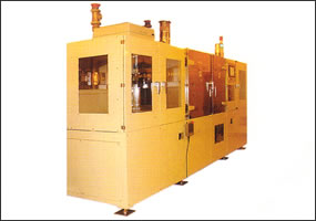
| ↑Click here. You'll see a big picture.↑ |
 |
|
| 【 Feature 】 |
| ・ |
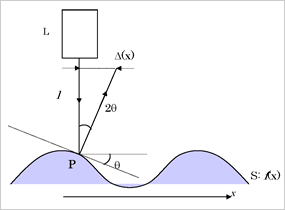
Non-contact inspection by laser. |
| ・ |
Ability to inspect by 0.1μm for a rough surface
0.1nm for a mirror (super smooth)surface. |
| ・ |
Vibration resistant (system does not require anti-vibration table), because of high speed scanning(0.52msec/30mm/1 line) |
| ・ |
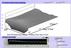
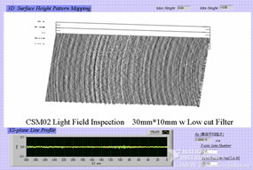
Ability to measure large areas, 30×30mm |
| 【 Application include 】 |
| ・ |
Super smooth surfaces such as a semiconductor, hard disk, LCD flat panel,
coated surfaces of many materials,and other typical metrological applications. |
| ・ |
Rough surfaces such as “ a copy drum”,textured surfaces,steps, and the such. |
| Angle of an object to be examined |
±4.3° |
| Laser |
Red semiconductor laser |
| Wave length |
650nm |
| Power |
Maximum 30mW |
| Class |
Class3B |
| Diameter |
φ25μm |
| Scan Length |
30mm |
| Scan speed |
30mm/0.52msec/line |
| Scan Height |
0.1nm |
| Scan Width |
25μm |
| Data Acquisition Speed |
8MHz |
Scanning time(30×30mm/
100μm"Pitch" /average 1 time) |
50sec |
| Average treatment times |
1〜99 times |
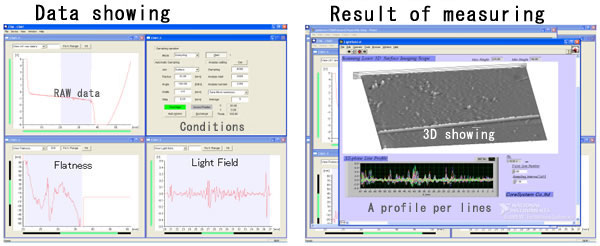
Showing
mode |
Flatness |
To examine flatness |
| Microwaviness |
To examine roughness |
| Light Field |
To examine slope |
X-Y-Rolling
positioning stage |
X axis |
±50mm ( 0.002mm "Pitch") |
| Y axis |
±50mm ( 0.002mm "Pitch") |
| Rolling axis |
360°( 0.01°"Pitch") |
| Indication |
A profile per lines
3D showing |
| Utility |
AC100V±15% / 15A |
| Weight (Equipment itself) |
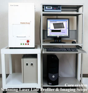
50kg |
|
|
| ↓Click here. You'll see a big picture.↓ |
 |
|
 |
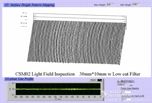
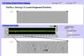
| An outside edge of a hard disk |
|
The surface of a hard disk (After putting on texture) |
 |
 |
 |
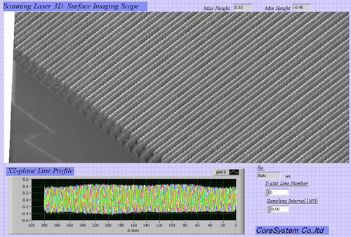
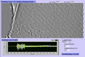
| A surface of Silicon Wafer |
|
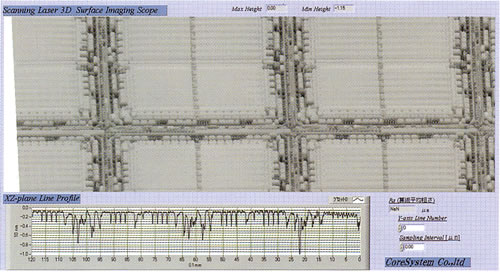
A surface of semiconductor pattern |
 |
|
 |
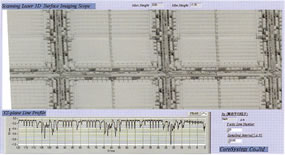
| A surface of a liquid panel |
|
A surface of a plasma display |
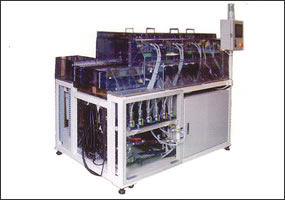
| ■LCD Cleaning System |
|
■LCD Carrier Cleaning System |
 |
|
 |
| 【 Features 】 |
| ・ |
Panel by panel cleaning by roll scrubbing |
| ・ |
High speed cleaning : 10sec/panel |
| ・ |
Ease of Maintenance |
| ・ |
Cleaning with no stress to the of Substrate |
|
|
| 【 Features 】 |
| ・ |
High speed cleaning : 8min/carrier |
| ・ |
Ease of Maintenance |
| ・ |
This system has self-cleaning |
|
| 【 Panel size capabilities 】 |
| CF: |
L(46.27〜182.75)×W(35.97〜137.1)
t=0.8〜2.2 |
| TFT: |
L(49.7〜186.6)×W(40.8〜142.5)
t=0.8〜2.2 |
|
|
| 【 Carrier size capabilities 】 |
| |
W333×D294×H420 |
|
|